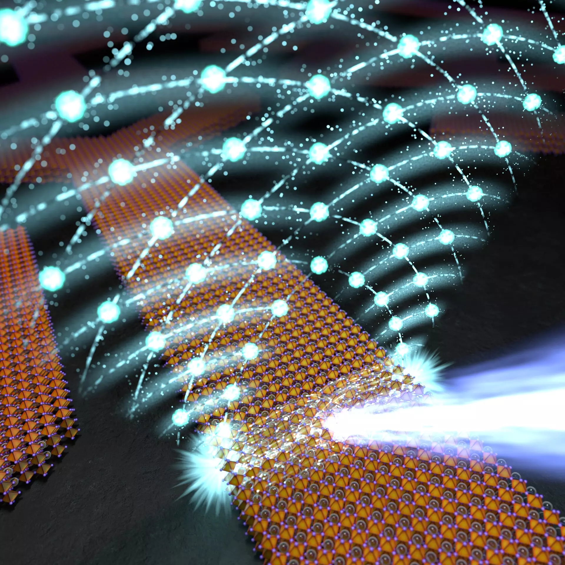
Recent advancements in the field of photonics have highlighted the potential of integrated photonic circuits, especially those that leverage room temperature operation combined with optical nonlinear effects. Researchers from the Faculty of Physics at the University of Warsaw, alongside collaborators from Poland, Italy, Iceland, and Australia, have pioneered a method for creating specially designed perovskite crystals that serve as vital components in nonlinear photonics applications. These remarkable structures possess the capacity to act as waveguides, modulators, couplers, and splitters, thus promising a broad spectrum of functionalities in both classical and quantum signal processing.
What’s particularly intriguing about perovskite materials, such as cesium lead bromide (CsPbBr3), is their versatility in shape and application. Professor Barbara Piętka, a key player in this research, emphasizes this versatility, noting that these crystals can be synthesized in various forms, from polycrystalline layers to nano- and micro-sized particles. The high exciton binding energy and strong oscillator strength in materials like CsPbBr3 allow for enhanced light interaction, which significantly lowers the energy thresholds required for nonlinear optical processes. This characteristic positions perovskites as ideal candidates for cutting-edge optical applications, encompassing areas as varied as solar technology and laser systems.
Central to the success of the research is the development of scalable, repeatable synthesis methods for these perovskite crystals. The team employed a microfluidic technique that facilitates the growth of the crystals within narrow polymer molds, allowing for precise control over dimensions and shapes. By carefully managing solution concentration and growth temperatures in a controlled atmosphere saturated with solvent vapors, researchers were able to grow exceptionally high-quality single crystals. The use of gallium arsenide templates, refined through electron-beam lithography and plasma etching, has enabled the production of crystals with intricate geometries, thereby expanding the design possibilities for integrated photonic devices.
A significant finding from this research involves the demonstration of polaritonic lasing—a phenomenon arising from the interactions between exciton-polaritons. These quasiparticles exhibit unique properties that blur the lines between light and matter. The research team observed the lasing effect arising from the edges and corners of the microwires, which is indicative of strong light-matter interactions and the creation of a non-equilibrium Bose-Einstein condensate. Unlike traditional lasing where emissions are influenced by the Purcell effect, this new approach signifies a leap into operating conditions characterized by strong coupling.
Dr. Helgi Sigurðsson highlighted the confirmation of coherence among emitted light signals, reinforcing the significance of the polariton condensate’s macroscopically extended nature. This coherence opens up avenues for enhanced signal processing capabilities, crucial for both classical and quantum applications.
The implications of the research extend into the realm of nonlinear optics, where the observations of blueshifts, indicating increasing energy correlating with population density in a given mode, signal the rich interactions within the condensate. This effect is critical as it facilitates long-range propagation of light, enabling the emitted signal to travel through air gaps to adjacent structures. These interactions also verify the potential of utilizing perovskite structures in developing compact computational systems that manage both classical and quantum tasks.
As the researchers project into the future, the integration of these innovative materials with existing silicon-based technologies emerges as a key focus. The compatibility of perovskite structures with silicon suggests a promising pathway toward commercialization—a crucial step for translating scientific breakthroughs into practical applications. Professor Michał Matuszewski’s optimism about developing devices capable of operating at the single-photon level fosters hope for the emergence of integrated photonic circuits that merge nanolasers, waveguides, and other essential components on a single chip.
The ongoing research into perovskite crystals represents a synchrony of materials science, photonics, and quantum technology. The versatile nature and scalability of these structures position them as transformative assets in nonlinear photonics. As researchers continue to explore and refine these materials, their anticipated integration into broader technological frameworks may very well usher in a new era of optical technologies, enhancing both the capacity for advanced computation and the overall functionality of photonic systems. With these developments, we stand on the cusp of significant innovation in how we process and transmit both classical and quantum signals.
Leave a Reply