The field of electronic components is constantly evolving, with researchers always on the lookout for materials that could revolutionize the industry. Two-dimensional (2D) semiconducting materials have emerged as promising candidates due to their unique optoelectronic properties. However, effectively integrating these materials with gate dielectrics has posed a challenge, leading to degraded transistor performance. Recently, researchers at King Abdullah University of Science and Technology (KAUST) and Soochow University, among others, have introduced a novel approach that could pave the way for the development of improved transistors based on 2D semiconductors.
The team’s innovative design involves the use of hexagonal boron nitride (h-BN) dielectrics and metal gate electrodes with high cohesive energy, such as platinum (Pt) and tungsten (W). By utilizing Pt as an anode, the researchers discovered that the h-BN stack was less likely to experience dielectric breakdown, resulting in significantly lower leakage currents and enhanced dielectric strength. This finding led them to explore the potential of chemical vapor deposited h-BN as a gate dielectric for 2D transistors.
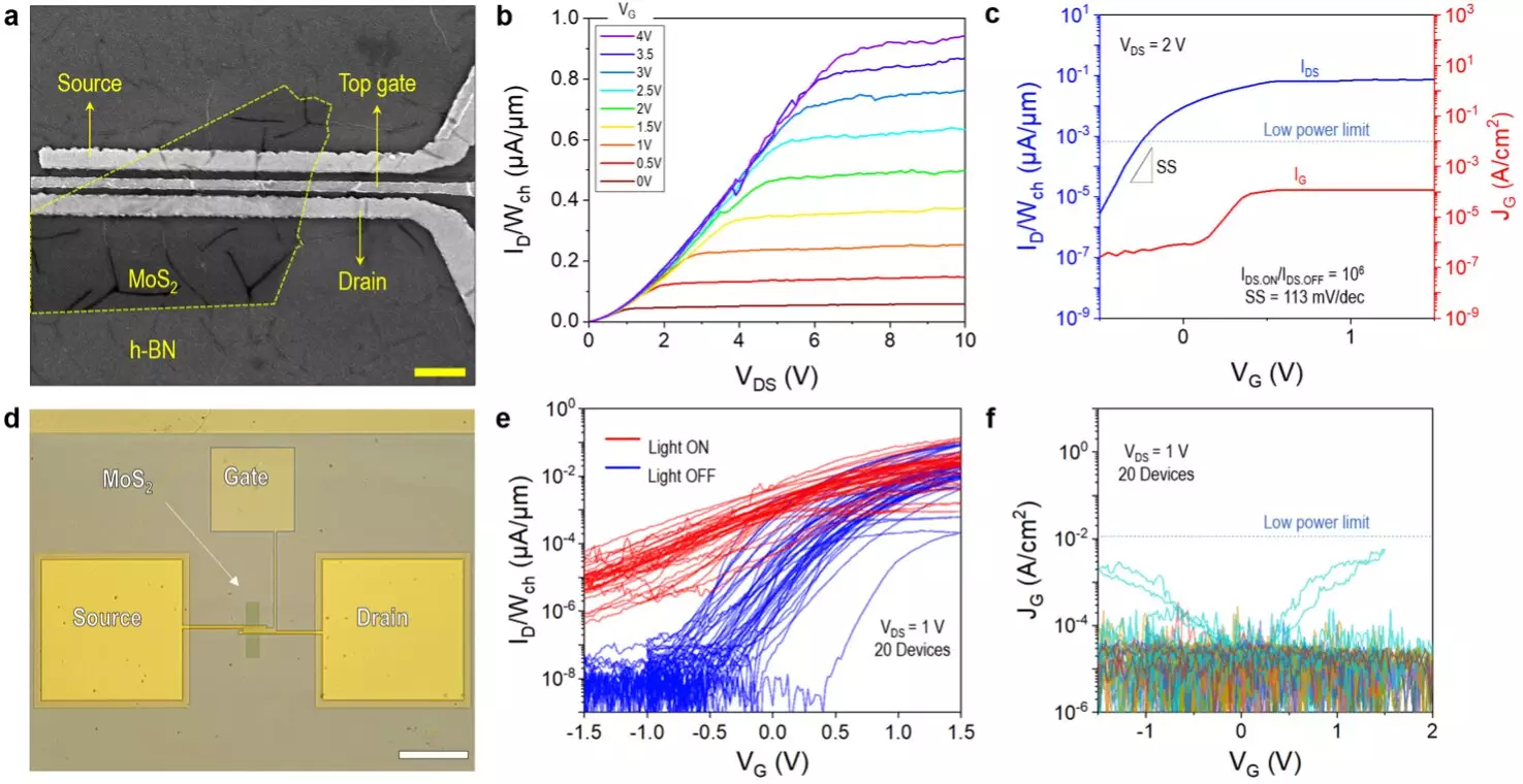
Through meticulous experimentation, the team fabricated over 1,000 devices incorporating h-BN gate dielectrics. The process involved layering h-BN films on a SiO2/Si substrate, patterning source and drain electrodes (Ti/Au) using electron beam lithography, and transferring MoS2 channels onto the electrodes. Subsequently, the Pt gate electrode was patterned and deposited using e-beam evaporation. The clean van der Waals interface between MoS2 and h-BN in the transistors played a crucial role in improving reliability and performance.
Contrary to common beliefs, the researchers demonstrated that CVD h-BN, when paired with high cohesive energy metals like Pt and W, could effectively function as a gate dielectric in 2D transistors. The integration of MoS2 and h-BN created a clean interface, enhancing the overall reliability of the devices. The team’s approach significantly reduced current leakage and achieved a high dielectric strength of at least 25 MV/cm, showcasing the potential of their method for future electronic components.
The successful fabrication of 2D semiconductor-based transistors using h-BN gate dielectrics opens up new possibilities for solid-state microelectronic circuits and devices. The team’s findings could potentially lead to the development of highly performing 2D semiconductor-based devices, with researchers across the globe exploring similar approaches and materials. As the research progresses, the team aims to create ultra-small, fully 2D transistors to contribute to the advancement of the industry and help extend Moore’s Law.
The integration of 2D semiconductor materials with appropriate gate dielectrics and metal electrodes represents a significant step forward in the field of electronic components. The team’s innovative approach not only improves the performance of transistors but also opens up avenues for further exploration and innovation in the realm of 2D materials. With continued research and development, 2D semiconductors could soon become a cornerstone of next-generation electronic devices, ushering in a new era of technology and innovation.


Leave a Reply