Semiconductors are fundamental to modern technology, serving as the backbone for everything from solar panels to microchips. This research, emerging from UC Santa Barbara, represents a groundbreaking advancement in our understanding of how electric charges—specifically photocarriers—move across interfaces in composite semiconductor materials. Utilizing innovative scanning ultrafast electron microscopy (SUEM), the study succeeded in visualizing this rapid process for the first time, expanding our knowledge beyond theoretical hypotheses and indirect observations traditionally seen in textbooks.
Associate Professor Bolin Liao leads the team behind this pivotal research. According to Liao, most traditional methods rely on indirect measurements that often leave gaps in our understanding of charge movement. “There are a lot of textbooks written about this process from semiconductor theory,” he noted, implying that while the theoretical framework is robust, the practical visual understanding has been sorely lacking. The current study, as published in the Proceedings of the National Academy of Sciences, not only addresses this gap but also serves as a benchmark for measuring the accuracy of existing theories.
Understanding how photocarriers—electrons and “holes” generated in semiconductors when exposed to light—travel through materials is crucial for developing efficient photovoltaic devices. The problem arises from the fact that these carriers lose significant energy in their journey across the material, losing vibrancy within picoseconds and converting useful energy into heat. Thus, a detailed characterization of their movement and behavior at heterojunctions can lead to more efficient designs that potentially mitigate energy losses.
Heterojunctions—interfaces between two different semiconductor materials—play a vital role in a myriad of applications including lasers, sensors, and enhanced energy conversion techniques. The researchers focused on a heterojunction formed by silicon and germanium, two well-known materials with significant applications in renewable energy and telecommunications. By using SUEM, they were able to witness for the first time the dynamic behavior of hot photocarriers as they traveled across this interface.
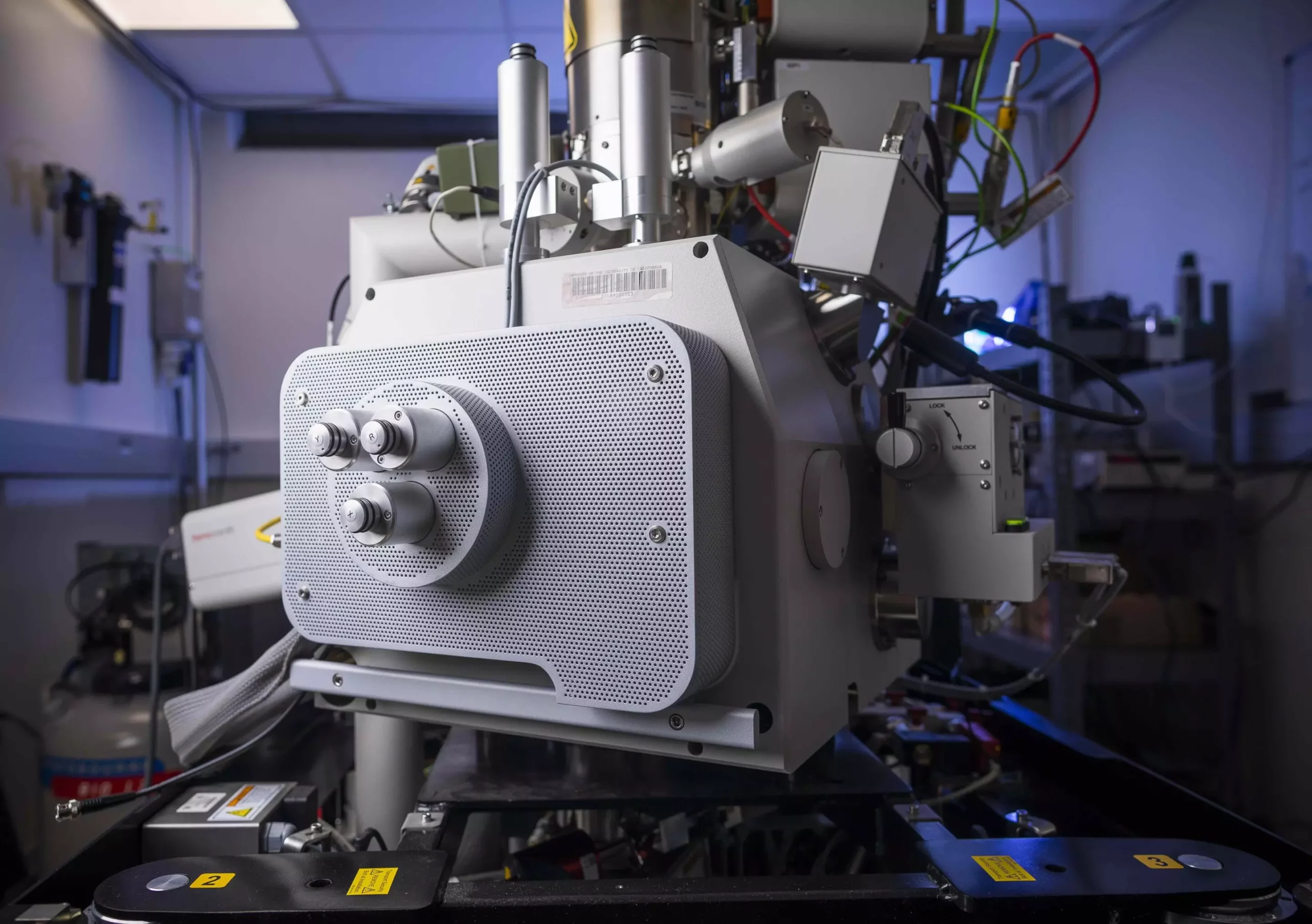
Liao described their method as an effort to integrate temporal resolution into traditional electron microscopy techniques. The SUEM process employs ultrafast laser pulses, acting as a picosecond-scale shutter for the electron beam that scans the surface of these semiconductor materials energized by optical pumps. As charges are generated through this exciting optical process, the research team could visualize their transient behavior within a timeframe ranging from picoseconds to nanoseconds.
What makes this breakthrough particularly fascinating is the unprecedented ability to observe how these charges diffuse across the junction from one semiconductor material to the other. The study revealed that while photocarriers excited in the uniform sections of silicon or germanium exhibited rapid movement due to their initial high energy, those generated close to the heterojunction faced a bottleneck. Many of these charges became trapped by the heterojunction potential, causing a reduction in their mobility and ultimately influencing device performance.
This qualitative observation opens new avenues for research within semiconductor design. Understanding that charge trapping can significantly impede the efficacy of energy harvesting devices poses a critical challenge for semiconductor engineers and designers. The findings underscore the necessity of addressing these trapping phenomena to enhance energy collection and device efficiency.
This research also pays homage to the foundational work of the late Professor Herb Kroemer, whose pioneering research laid the framework for modern semiconductor theory in the 1950s. Kroemer’s assertion that “the interface is the device” has now been vividly illustrated through the recent findings of the UCSB team. The visualization of hot photocarrier behavior at heterojunctions encapsulates the evolution of semiconductor research, bridging the gap between historic theories and contemporary technological applications.
The recent advancements performed at UC Santa Barbara signify a momentous step in semiconductor materials science. By directly visualizing the phenomenon of charge transfer at heterojunctions, researchers have not only validated existing theories but have introduced a crucial tool for future explorations in semiconductor technology. This ongoing work opens the door to optimizing energy conversion efficiencies and overcoming the challenges associated with hot carriers, leading to enhanced performance in a variety of electronic devices. As this field continues to evolve, the potential for transformative impacts on technology remains boundless.


Leave a Reply