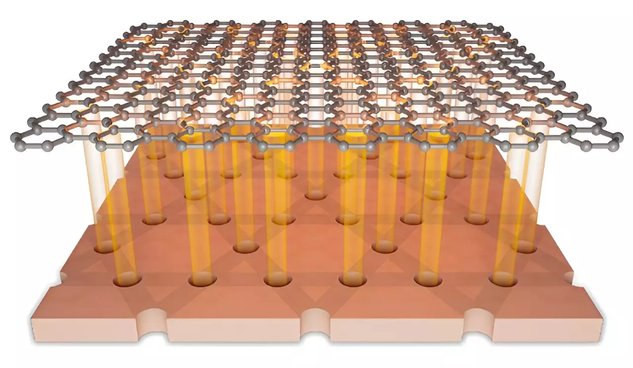
Controlling electronic band structures in materials such as graphene has long been a tantalizing goal for researchers. Traditional methods, including heterostructures, interfacial strain, and alloying, offer limited capabilities for in situ and continuous manipulation of band characteristics. The advent of van der Waals (vdW) materials, particularly graphene, has shifted the landscape, presenting new possibilities in band engineering. However, the core challenge remains: achieving precise, selective control over band structures to elicit desired electronic properties. This challenge has steered scientists towards innovative approaches, highlighting the need for enhanced methodologies that surpass the limitations of earlier techniques.
Introduction of the Kagome Superlattice
Recent research led by a team from the University of Science and Technology of China (USTC) has introduced a groundbreaking technique involving an artificial kagome superlattice for modulating the electronic properties of graphene. This innovative approach employs a lattice configuration with a remarkably large period of 80 nm, designed to manipulate the Dirac bands in graphene effectively. Unlike conventional methods, the kagome superlattice facilitates the folding of high-energy bands into lower energy states, making them amenable to experimental observation and manipulation.
The significance of this method lies not just in its design but also in its application. By constructing a high-order potential within the kagome superlattice, the researchers enable a unique form of band structure reconstruction that can selectively manipulate band dispersions. This advancement represents a fundamental shift in the way researchers can engage with band structure engineering.
The successful implementation of the kagome superlattice relied on standard vdW assembly techniques and high-precision electron beam lithography to produce a consistent kagome-lattice pattern. This pattern functions as a local gate for the graphene, allowing researchers to experiment with various electronic properties dynamically. By adjusting the voltage applied both to the local gate and the doped silicon substrate, the team demonstrated the capability to finely tune the artificial potential’s strength and the carrier density in the graphene material.
This dual-control strategy is particularly significant because it introduces a high degree of flexibility in manipulating electron interactions, thereby enabling researchers to explore a diverse array of electronic configurations. The ability to observe and adjust spectral weight redistribution among multiple Dirac peaks underlines the potential of this technique for both fundamental studies and practical applications in electronic devices.
Another vital aspect of this research is the role of magnetic fields in influencing the band structure alterations induced by the kagome superlattice. When a magnetic field is applied, it effectively diminishes the superlattice’s modulation effects, reinstating the intrinsic Dirac band characteristics. This finding not only illustrates the multifaceted nature of electronic behavior in graphene but also provides an additional lever for tuning electronic properties.
The interplay between the kagome superlattice and external magnetic fields exemplifies the complexity of controlling band structures and suggests potential pathways for creating devices that exhibit tunable electronic characteristics under varying external conditions.
The methodology and findings detailed in the study hold broad implications for the field of material science, specifically in the realm of band structure engineering. By providing a new mechanism for conducting precise electronic property manipulations, this research could pave the way for innovations in developing materials with tailored functionalities. Such advancements could have far-reaching impacts on various technological domains, including next-gen electronic devices, sensors, and potentially quantum computational elements.
The collaborative efforts of esteemed researchers from USTC, Wuhan University, and IMDEA Nanociencia signify a potent convergence of expertise that not only enhances the credibility of these findings but also fosters an environment ripe for future discoveries in material engineering.
The introduction of an artificial kagome superlattice represents a significant leap forward in the field of band structure engineering. By empowering researchers with unprecedented control over electronic properties, this method encourages further exploration and experimentation. As we stand on the cusp of a new era in material science, the potential for discovering novel phenomena and functionalities in engineered materials continues to expand, promising exciting advancements in both scientific research and practical applications.


Leave a Reply