Antiferromagnetic materials are a class of substances where the magnetic moments of adjacent atoms align in a staggered configuration. This arrangement leads to a cancellation of their magnetic fields, thereby resulting in no net magnetism at a macro level. These fascinating materials have drawn significant attention in recent years due to their potential applications in advanced electronics and spintronics—a field that exploits the intrinsic spin of electrons rather than their charge for information processing. Researchers at Harvard University have made exciting strides in this area by investigating the antiferromagnetic diode effect in the even-layered manganese bismuth telluride (MnBi2Te4).
Their findings, published in the journal Nature Electronics, reveal a novel capability of MnBi2Te4, a centrosymmetric antiferromagnet, to exhibit a diode effect—a phenomenon traditionally associated with the flow of current in one direction within a device. This research is pivotal because it indicates that effective charge transport can be achieved without the directional charge separation typically found in non-centrosymmetric materials. The researchers noted that this attribute opens up new avenues for creating innovative electronic devices such as in-plane field-effect transistors and systems for harvesting microwave energy.
Much of the original discourse around the diode effect has largely been dominated by materials with a more complex structural symmetry. However, the team at Harvard, comprising Anyuan Gao, Shao-Wen Chen, and their colleagues, shifted the focus toward the antiferromagnetic systems, exploring their unique characteristics. Their inquiry was framed within a broader context of analogous effects observed in non-centrosymmetric superconductors, ultimately leading to the unexpected discovery of a similar effect in MnBi2Te4.
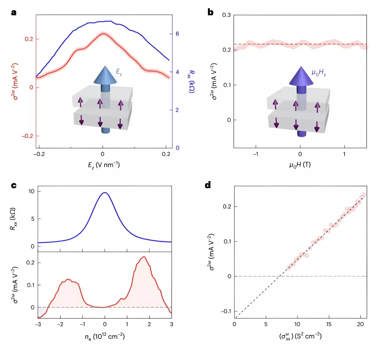
To investigate this phenomenon, the researchers engineered various device configurations using MnBi2Te4. They employed distinct electrode arrangements, including Hall bar electrodes, which measure the Hall effect through a longitudinal current, and radially distributed electrodes for potential variation analysis. Remarkably, both configurations illustrated an antiferromagnetic diode effect, displaying nonlinear electrical transport patterns.
The research team utilized a combination of techniques to extract meaningful insights, including spatially resolved optical methods and electrical sum frequency generation (SFG) measurements. Their methods confirmed the presence of significant second-harmonic transport behavior, thus substantiating their findings. This nonlinear transport is a hallmark of the antiferromagnetic state present in the layered structure of MnBi2Te4, showcasing its potential to revolutionize how we conceptualize electronic device architecture.
The implications of the antiferromagnetic diode effect are vast and impactful. Beyond the immediate applications in creating more efficient field-effect transistors and microwave energy harvesting devices, the findings hint at a promising future for antiferromagnetic logic circuits and spintronic systems that transcend the limitations of conventional charge-based electronics. The observed phenomena could pave the way for enhanced data processing speeds and reduced power consumption, essential characteristics for next-generation electronic components.
Furthermore, the authors of the study emphasize that their discovery is merely the tip of the iceberg. There is an expansive realm of exploration ahead regarding the antiferromagnetic diode effect, which could lead to the development of high-performance, innovative electronic devices. Future studies will likely delve deeper into how these materials can be manipulated to create advanced functionalities.
In essence, the work conducted by the Harvard team on the antiferromagnetic diode effect in MnBi2Te4 highlights a remarkable turning point in material science and electronics. This study not only illustrates the complex interplay between magnetism and electric transport in antiferromagnetic materials but also sets the stage for future innovations in spintronics and related fields. With continued exploration and experimentation, we may soon witness transformative technologies that redefine our interaction with electronic devices, making them faster, more efficient, and fundamentally different from their predecessors.


Leave a Reply