In the ever-evolving sphere of materials science, significant advancements are a norm, but few breakthroughs resonate as powerfully as the recent achievements at the University of Chicago. Researchers led by Assistant Professor Sarah King have made headway in the imaging of antiferroelectric materials—substances whose unique electrical characteristics present a landscape brimming with potential applications in energy storage, sensors, and memory technologies. Not merely a technological feat, this innovation holds the key to unlocking materials’ hidden attributes and maximizing their capabilities.
The importance of imaging the electronic properties of materials becomes increasingly apparent as technology advances. Institutions face mounting pressures to not only innovate but also to refine existing technologies for specific uses. King’s lab triumphantly overcomes longstanding challenges in material characterization, paving the way for future innovations. The presence of antiferroelectric materials in this new discourse is pivotal; these materials, with their unique configurations of electric dipoles, embody an untapped potential that scientists have struggled to fully grasp.
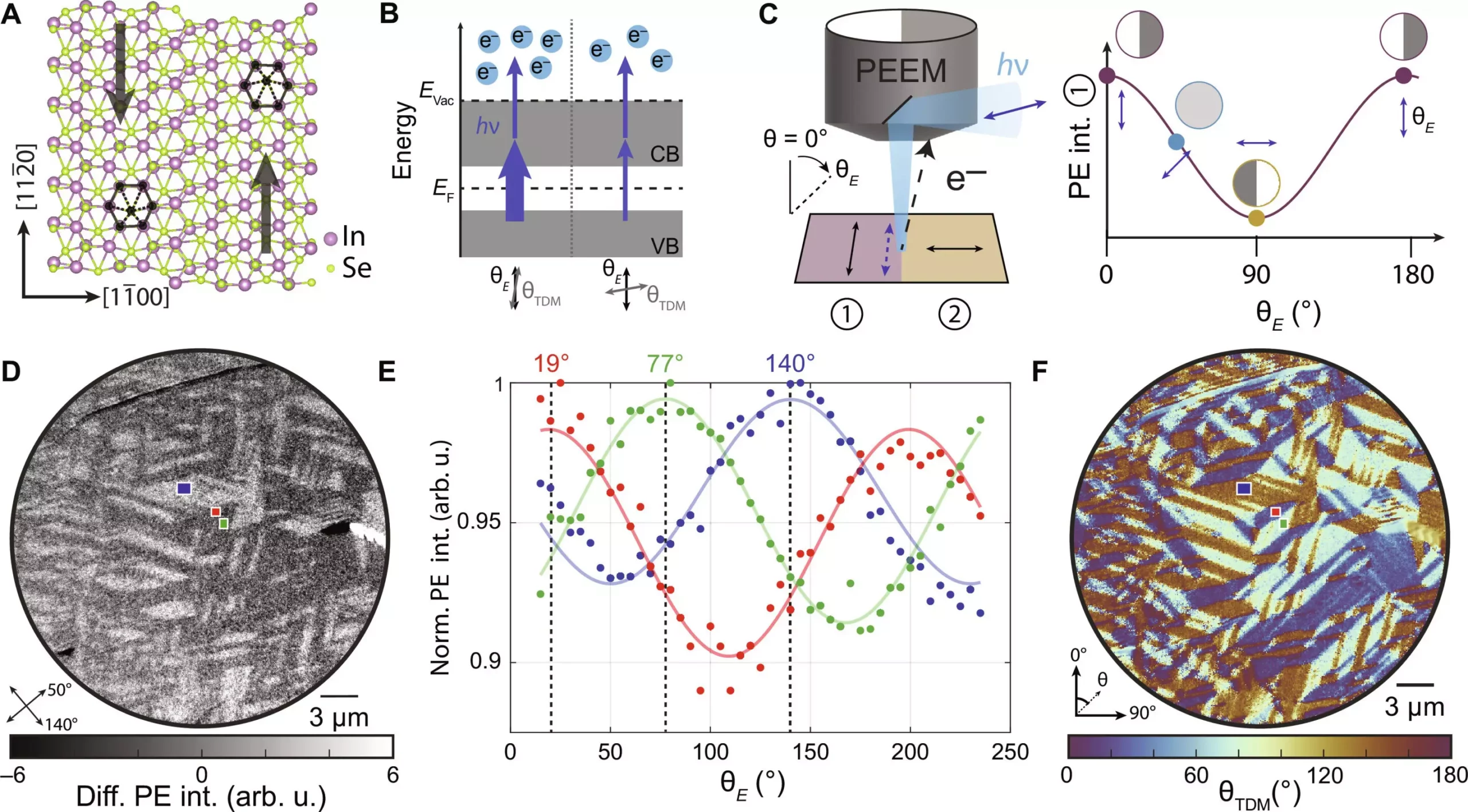
A Breakthrough in Imaging Techniques
The introduction of this new imaging method, highlighted in a study published in *Science Advances*, fundamentally shifts how researchers interact with antiferroelectric materials. The importance of having high spatial resolution in imaging techniques cannot be overstated; it is a game-changer in a field where many conventional methods have faltered. King emphasizes this transformative capacity: “Having new imaging techniques with such high spatial resolution is incredibly powerful,” she states, underscoring the anticipation surrounding the implications of these advancements on future material development.
Traditional imaging methods have historically lacked the precision required to visualize the intricate domains within antiferroelectric materials. This limitation has stymied understanding, as the ability to see how electric dipoles align—or misalign—can inform entire fields, from nanotechnology to sustainable energy solutions. King’s lab utilized polarization-dependent photoemission electron microscopy, a novel technique that allows researchers to probe deeply into the electronic properties and interfaces within materials. By combining the precise polarized light from lasers with electron imaging, scientists can now create a detailed map of the nanoscale arrangements of domains within materials like indium selenide, hitherto shrouded in mystery.
Anticipating Transformative Applications
This newfound capability to visually analyze the domains of antiferroelectric materials illuminates far more than basic scientific curiosity; it holds transformative implications for practical applications in electronics and energy storage. Antiferroelectric materials offer fascinating properties—in essence, they display the duality of canceling electric polarization while potentially transitioning to states of higher energy. This cut-and-dry property could redefine technologies ranging from ultra-efficient energy storage systems to sensors with unprecedented sensitivity.
Researchers foresee a future where these materials are fine-tuned and tailored for specific tasks, harnessing their unique switching capabilities to develop innovative devices. Sarah King’s vision extends into the heart of materials science, where understanding domain switching and further exploration of phase transitions could become common pursuits. The dynamic between order and disorder plays a crucial role in materials development, and with new imaging methods, researchers can now dissect this relationship with unprecedented clarity.
Interdisciplinary Collaboration and Advancements
This achievement is not merely an isolated success; it embodies the collaborative ethos within the scientific community. King’s team—comprising undergraduate and graduate students, as well as postdoctoral researchers—demonstrates the power of combined efforts across various academic stages and disciplines. Their commitment to advancing knowledge in materials science does not just benefit them; it opens a dialogue across the field, fostering collaborations that could lead to revolutionary applications.
In an age defined by rapid technological advancement, the implications of such findings cannot be ignored. With ongoing research and collaboration bolstered by these imaging breakthroughs, the potential applications of antiferroelectric materials could soon transcend theoretical discussions and enter the realm of practical solutions—solutions that promise to enhance energy efficiency and environmental sustainability in myriad industries. The future of materials science looks brighter than ever, and the University of Chicago is at the forefront of this exciting revolution.
Leave a Reply